News

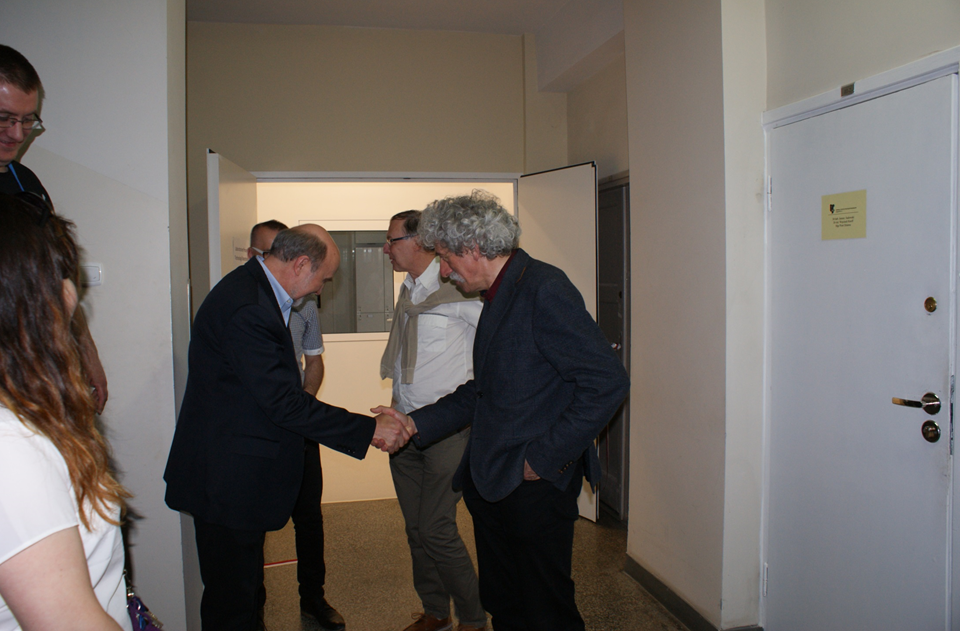
Just after the ribbon cutting ceremony in front of the Lab entrance, Dr Tomasz Wojciechowski and Prof. Tomasz Wojtowicz accepted congratulations front the Director of the Institute of Physics, Prof. Roman Puźniak, and from the President of the International Research Foundation MagTop, Prof. Tomasz Dietl, on the occasion of the successful realization of two large investment projects from the Ministry of Sciences and Higher Education, which led to the creation of the new Laboratory.
On 23rd May 2017 Dr. Tomasz Wojciechowski and Prof. Tomasz Wojtowicz from MagTop and the Institute of Physics, Polish Academy of Sciences gave a talk entitled “Capabilities of the new Laboratory of Technological Processes of Semiconductor Nanostructures and Devices” at the Condensed Matter Seminar of the Institute.
On 23rd May 2017 Dr Tomasz Wojciechowski and Prof. Tomasz Wojtowicz from MagTop and the Institute of Physics, Polish Academy of Sciences gave a talk entitled “Capabilities of the new Laboratory of Technological Processes of Semiconductor Nanostructures and Devices” at the Condensed Matter Seminar of the Institute (see presentation in Polish language). The seminar was part of an official ceremony of opening of the new Interdivisional Laboratory of the Institute. Just after the seminar the Director of the Institute, Prof. Roman Puźniak, performed a ribbon cutting ceremony, followed by coffee and cake party. MagTop has plans of using this new clean room facility equipped with cutting edge apparatus for the realization of its research plans. It is worth mentioning that Dr Wojciechowski has played a leading role in creation of this new Lab, starting from preparing successful applications for funds, through organizing pubic tender procedures for purchasing equipment and ending with launching the operation of the Lab. One can take a virtual tour of the Laboratory here.
Tabs: Laboratoria\Nanotechnologia and: _MBE: II-VI (Molecular Beam Epitaxy of II-VIs and of new topological materials); _Metalizacja1 (UHV deposition of metals); _Fotolitografia (Photolithography); _ALD, RIE, PECVD (ALD – Atomic Layer Deposition, Chlorine-based ICP-RIE – Inductively Coupled Plasma Reactive Ion Etching, ICP-PECVD – fluorine-based Inductively Coupled Plasma – Plasma Enhanced Chemical Vapour Deposition).