MagTop’s and VIGO Photonics’s R&D teams examined theoretically optical characteristics of semiconductor quantum superlattices (SL) of III-V compounds. Extensive collaboration concerned also contact and etching properties of detector structures. Furthermore, a new class of highly perspective detectors, combining advantages of II-VI and IV-VI compounds was developed at MagTop.
 |
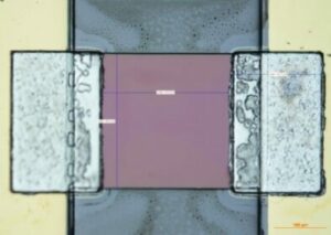 |
Modern applications in the field of mid- and long-wavelength infrared (detection, such as thermal imaging cameras or investigation of zero-gap topological matter, require sensitive, high-speed detectors. In the frame of collaboration agreement signed MagTop’s and VIGO R&D teams carried out a theoretical study of the electronic and optical properties of III-V SLs within the framework of relativistic density functional theory [1], which should help in design more sensitive detectors. On the experimental side, MagTop’s MBE Group collaborated with VIGO on various aspects of optimizing detector design, its testing, contacts, and etching.
MagTop has also worked on the IR detectors based on narrow gap IV-VI semiconductors, whose sensitivity is limited by the processes of non-radiative recombination of photo-excited carriers by the Auger relaxation process. This limitation can be minimized by building detectors based on multilayer structures containing quantum wells made of IV-VI and wide band gap semiconductors, since the effect of Auger recombination processes on the device performance is much weaker in wide-gap materials. However, in narrow/wide-gap semiconductor systems, the component materials usually have significantly different refractive indices, so photonic effects must be taken into account in the device design, as they can significantly improve or reduce the final detector performance.
MagTop’s Weyl Group, in cooperation with IFPAN, proposed a new solution for IR detectors based on superlattices made of IV-VI narrow gap PbTe and II-VI wide gap CdTe. MagTop’s Michał Szot, guided by the results of his research conducted partly within the framework of “Innovation Incubator 4.0”, designed several structures of the optically active area of the infrared detector manufactured by MBE, taking into account the photonic effects. Based on these structures, VIGO, using industrial processing methods, has built and successfully tested a series of prototype detectors operating in the wavelength range from 1 to 4 µm. In addition, M. Szot is currently preparing two patent applications for new types of infrared detector with a tunable detection wavelength.
[1] G. Hussain, G. Cuono, R. Islam, A. Trajnerowicz, J. Jureńczyk, C. Autieri, T. Dietl, Electronic andoptical properties of InAs/InAs0.625Sb0.375superlattices and their application to far-infrared detectors, J. Phys. D: Appl. Phys. 55, 495301 (2022).
Collaboration agreement between VIGO and MagTop/IFPAN was signed on 24 October 2019.
Thermoelectric generators and coolers are semiconductor devices that directly convert heat into electricity (thermoelectric generators – TEGs) or vice versa (thermoelectric coolers – TECs) using the ability of electrons to simultaneously transfer heat and electric charge. Thermoelectric devices with sufficiently high energy conversion efficiency could become a technological solution in the worldwide search for electron systems that efficiently harvest waste industrial heat. MagTop’s and PUREMAT Technologies’s researchers developed nanocomposite PbTe-CdTe in which enhanced thermal resistance is not compromised by the deterioration of electrical conductivity.
 |
A good thermoelectric material should possess high electric conductivity and high Seebeck coefficient S (thermoelectric power) but very low thermal conductivity. IV-VI narrow gap semiconductors and their alloys, like Pb1-xSnxTe, are well-known thermoelectric materials. In particular, PbTe and wide gap CdTe constitute an ideal materials platform for researching both conventional and new strategies of improving conversion efficiency, like alloying for band structure engineering or nanostructuring. At IFPAN, we manufacture PbTe-CdTe semiconductor materials in a variety of forms: bulk monocrystalline ternary solid solutions Pb1-xCdxTe, heavily doped bulk polycrystals PbTe-CdTe with two crystalline phases (rock-salt PbTe and zinc-blende CdTe) as well as low-dimensional layered heterostructures grown by molecular beam epitaxy method. Nanostructuring implies preparation of herostructures based on good thermoelectrics or introducing into them nano- and micro-grains of the same or other material phases. Based on our recent experimental and theoretical studies of electron and heat transport in monocrystalline Pb1-xCdxTe grown from the vapor [1] as well as exploiting a very low mutual solubility of PbTe and CdTe, we developed a versatile practical procedure of producing a bulk PbTe-CdTe thermoelectric nanocomposite for the use in thermoelectric generators operating at temperatures T = 600¸800 K [2]. Structural properties, electrical conductivity, thermoelectric power and thermoelectric figure of merit ZT parameter were experimentally determined for PbTe-CdTe nanocomposites with a Cd content of up to 10 at.%. Developed in cooperation with IFPAN spin-off company PUREMAT Technologies and protected by the European patent [3], the method enables the control of electric conductivity of the composite by doping with acceptors (Na) or donors (Bi, I) and also control of the size and spatial distribution of CdTe precipitates in PbTe matrix (see Figure).
[1] M. Szot, P. Pfeffer, K. Dybko, A. Szczerbakow, L. Kowalczyk, P. Dziawa, R. Minikayev, T. Zajarniuk, K. Piotrowski, M. U. Gutowska, A. Szewczyk, T. Story, and W. Zawadzki, Two-valence band electron and heat transport in monocrystalline PbTe-CdTe solid solutions with Cd content up to 10 atomic percent, Phys. Rev. Materials 4, 044605 (2020).
[2] M. Szot, K. Dybko, A. Mycielski, A. Reszka, R. Minikayev, P. Dziawa, T. Story, Thermoelectric PbTe-CdTe bulk nanocomposite, arXiv.2212.14616.
[3] European Patent nr EP4036057A1: M. Szot, K. Dybko, T. Story – MagTop/IF PAN, and A. Mycielski – PUREMAT/IF PAN; European Patent Bulletin 49 (2022).
Collaboration Agreement between PUREMAT Technologies and MagTop/IFPAN was signed on October 30, 2019
Magnetron sputtering is an industry and research-relevant high-rate vacuum coating technique that allows the deposition of many types of materials, including metals and ceramics, onto as many types of substrate materials by the use of a specially formed magnetic field applied to a diode sputtering target. This method is also being used by MagTop’s researchers to deposit ferromagnetic metals, resulting in an invention now used by the PREVAC company in its products.
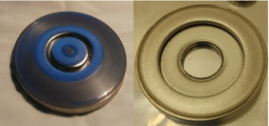
Sputtering ferromagnetic materials, for example, to interface magnetism with topological matter – which is one of MagTop’s goals – has proven challenging with commercially available sputtering sources. The problem is that the target shields the magnetic field and it is difficult to obtain a magnetic field of sufficient strength. Additionally, suboptimal field distribution above the target results in a non-uniform plasma distribution during the operation, resulting in turn in the need to frequently replace the target, which is not fully utilized and must additionally be thinner than 1.3 mm in case of iron (see Figure). Worse, it also leads to a flux that is not constant during the process.
The MagTop (MBE group)/PREVAC team proposed a solution to this problem through a special design of magnetic cores that not only provide a magnetic field that is parallel to the target’s surface and has sufficient strength, but is also obtained in a configuration that allows its safe cooling. Proof of concept was provided by an experimental demonstration carried out using a prototype source manufactured by PREVAC Ltd. that a much thicker magnetic target (up to 6 mm) can now be used and a much larger target volume can be utilized (see Figure). Critical from a technological point of view is the achieved long-term stability of deposition rate of ferromagnets.
As a follow up of the Agreement between PREVAC and IFPAN/MagTop, a patent application was submitted [1]. In the mentioned agreement, MagTop granted PREVAC the right, against payment, to use the invention in a new line of two inch sputtering sources manufactured by this company.
1] European Patent Application: Andreas Glenz (PREVAC), Krzysztof Fronc (International Research Centre MagTop) and Michał Chojnacki (Institute of Physics, Polish Academy of Sciences), Device for magnetron sputtering from target, EP22461556.7 (pending, submitted June 08, 2022).
Agreement on joint rights to a patent and joint patent between PREVAC sp. z o. o. and IFPAN representing MagTop was signed on October 19, 2021.
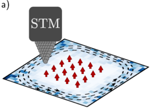
One of the emerging fields of the deep-learning methods is the development of qualitatively new protocols for drawing relevant and unbiased information from ever increasing volume of experimental data. MagTop’s researchers in collaboration with other groups, particularly with Bosch Center for Artificial Intelligence, proposed a machine-learning approach for classifying the topological states of 2D chiral superconductors and insulators based on local density of states data that can be obtained by scanning tunneling microscopy or possibly by nanoARPES. The developed new protocol can be applied to many experimental platforms that share qualitative features of the Shiba lattice models.
 |
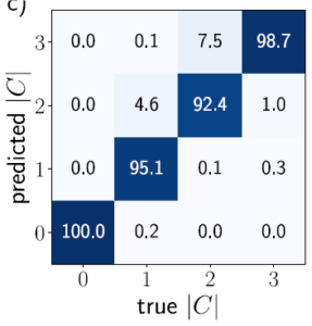 |
Scanning tunneling microscope provides LDOS data for the Shiba lattice (left panel). Confusion matrix (right panel) show accuracy of Chern number identification (in %) based on simulated LDOS data for a Shiba lattice model. All Chern numbers are predicted with the high accuracy. |
The fascination with topological materials and their potential for quantum technologies has led to a focus on achieving topological superconductors and their unique Majorana excitations. However, determining the topological properties of superconductors using existing experimental methods is a significant challenge. This challenge has become more pressing with the emergence of designer platforms that exhibit complex topology and are better suited for local probe techniques. To address this issue, we proposed a machine-learning approach for classifying the topological states of 2D chiral superconductors and insulators based on local density of states (LDOS) data. In 2D topological insulators and superconductors with time-reversal symmetry breaking, topological states are classified by an integer-valued Chern number. Determining the topological state requires identifying this number, which differs from insulators where it determines quantized Hall conductance. The challenge lies in quantizing thermal Hall conductance, which remains elusive. Although naturally occurring 2D topological superconductivity is uncertain, lab evidence supports its realization. Designer platforms, like the Shiba lattice, i.e., a system of magnetic impurities in a superconductor, exhibit topologically distinct phases. Experimental studies suggest a Chern number C of approximately 20, yet its confirmation lacks a diagnostic tool.
In our numerical experiments, we showed that an ensemble of neural networks, trained using generic tight-binding Hamiltonians, can identify the topological phases with |C| = 0, 1, 2, 3 in a representative part of the Shiba lattice model phase diagram, away from the phase boundaries, correctly with an average probability of > 96% (Figure). Since the LDOS can be measured with standard experimental techniques, such as scanning tunnelling spectroscopy and possibly nanoARPES, our protocol constitutes an important step in overcoming the long-standing problem of identifying the topology of 2D superconductors. The key advantage of our method is that, in the generation of the training data, we only need very rough information on the Hamiltonian corresponding to the system of interest. This allows us to parametrize a distribution of training models which covers the low-energy physics of this system as a special case.
[1] P. Baireuther, M. Płodzień, T. Ojanen, J. Tworzydło, and T. Hyart, Identifying Chern numbers of superconductors from local measurements, arXiv:2112.06777; under revision in SciPost Physics.
European Patent Application: P. Baireuther, M. Płodzień, T. Ojanen, J. Tworzydło, and T. Hyart, Device and Method for Indirect Measurement of Topological Invariants, EP21209049.2 (pending);
Join Invention Agreement between Robert Bosch GmbH and IFPAN representing MagTop was signed on March 3rd, 2022.